Avicena Unveils LightBundleTM, a Chip Interconnect Technology With Dramatically Lower Power Consumption and Higher Bandwidth Density
Avicena Unveils LightBundleTM, a Chip Interconnect Technology With Dramatically Lower Power Consumption and Higher Bandwidth Density
Highly parallel optical links with power efficiency of 0.1pJ/bit, bandwidth density of 10Tbps/mm2 and reach of up to 10m promise to smash current interconnect bottlenecks in distributed compute systems
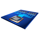
MOUNTAIN VIEW, Calif.--(BUSINESS WIRE)--Avicena Inc., a privately held company in Mountain View, CA, today unveils LightBundleTM, a highly parallel optical interconnect technology targeting up to 10 meters reach for chip-to-chip interconnects in distributed computing, processor-to-memory disaggregation, and other advanced computing applications. LightBundleTM is based on arrays of novel GaN high-speed micro-emitters, leveraging the microLED display manufacturing ecosystem, and is fully compatible with high performance silicon ICs.
Interconnects are becoming the key bottleneck in compute and network systems. Highly variable workloads are driving the evolution of densely interconnected, heterogeneous, software-defined clusters of CPUs, Graphical Processing Units (GPUs), Data Processing Units (DPUs) and shared memory blocks. Exploding Artificial Intelligence (AI) and Machine Learning (ML) workloads are exemplary of emerging applications driving an accelerating need for interconnects with extremely high density, low power consumption and low latency.
About the Technology
Today’s high-performance ICs use SerDes-based electrical links to achieve adequate IO density. However, the power consumption and bandwidth density of electrical links degrade quickly with length. Because optical interconnects do not have these same limitations, they have long been the prime contender to replace electrical interconnects for inter-chip communications. Unfortunately, conventional optical technologies (typically designed for networking applications) have been impractical for inter-processor and processor-memory interconnects due to their low density, high power consumption, inability to tolerate the high operating temperature of ASICs, and high cost.
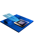
“All of this is changing with the recent advances in optical emitter technology driven by advances in the display industry,” says Bardia Pezeshki, founder and CEO of Avicena. “We have developed very high-performance optical transmitters based on emitter technology from the display industry. These innovative devices would have been impractical just a few years ago. Our optimized devices and materials support 10Gbps links per lane over -40°C to +150°C temperature with excellent reliability. We refer to our new optical sources as Cavity-Reinforced Optical Micro-Emitters or CROMEs. We connect CROME arrays with CMOS compatible PDs using multi-core fiber bundles to create massively parallel interconnects with 1000s of parallel lanes over a reach of up to 10m. We call this new class of optical interconnect the Avicena LightBundleTM.”
Avicena just demonstrated an array of 200 CROME devices with a pitch of 30μm coupled to an array of PDs with a multi-core imaging fiber. Individual lanes show excellent performance characteristics up to a data rate of 10Gbps over the full temperature range of -40°C to 150°C. This extrapolates to an aggregate link bandwidth of 2Tbps for 200 lanes with a bandwidth density of 10Tbps/mm2.
The parallel nature of the LightBundleTM technology is well-matched to parallel chiplet interfaces like AIB, HBI, and BoW, and can also be used to extend the reach of standard compute interconnects like PCIe, NVLink, and multi-channel G/DDR memory links with low power and low latency.
“The cloud and high-performance computing community has long recognized the value of a new class of interconnects,” said Bill Dally, Chief Scientist, NVIDIA. “Avicena’s technology has the potential to provide large improvements in power efficiency, bandwidth density, and reach.”
If you wish to learn more about the Avicena technology, here is a list of upcoming events:
Avicena at OFC 2021:
- Post deadline Paper Session, Fri. June 11, 8 – 10 a.m. PDT, B. Pezeshki et al., “Wide and parallel LED-based optical links using multi-core fiber for chip-to-chip communications”
- Rump Session, Wed. June 9, 6 – 8 a.m. PDT, C. Pfistner, “Slow & Parallel Minimizes Cost & Power”
Avicena cover story in the June 2021 edition of Compound Semiconductor Magazine:
- Compound Semiconductor, Volume 27, Issue IV 2021, B. Pezeshki et al., “Easing the chip-to-chip communication bottleneck by leveraging microLED display technology”
About Avicena
Avicena Inc. is a privately held company located in Mountain View, CA, specializing in the development of next-generation chip-to-chip interconnects that are more power efficient, offer higher bandwidth density and support longer reach than any current optical or electrical solution. Avicena’s technology is a key building block in the evolution of new compute architectures that will reduce the energy impact on our planet.
Contacts
Sama Pourmojib
sama@avicena.tech