DRESDEN, Germany--(BUSINESS WIRE)--Novati Technologies Inc., a leading global nanotechnology development center, today announced the availability of the industry’s most advanced Integrated Sensor Platform, placing a wide variety of sensors onto multi-layer stacks of wafers in order to consume less power and perform significantly faster while reducing overall footprint. Already proven for customer devices at Novati’s commercial development and manufacturing center, the platform paves the way for stacking single or multiple sensors with a broad selection of popular – as well as emerging – substrate materials, enabling new high-end applications for markets that include medical, semiconductors, photonics, security and aerospace.
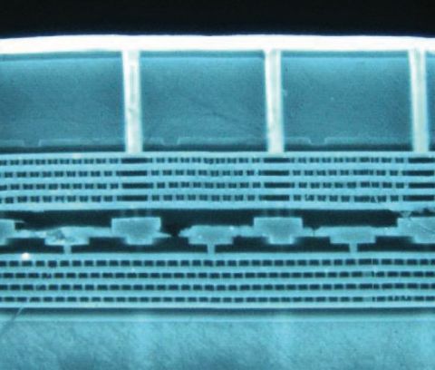
Demonstrating a version of this capability for high-performance computing, Novati last month jointly announced with Tezzaron Semiconductor the industry’s first eight-layer 3D IC wafer stack containing active logic, which controls the memory layers. The transistor and interconnect densities per cubic millimeter were far higher than achievable with 2D 14nm silicon fabrication, representing the densest 3D IC ever reported. Not limited to the high-end markets served by that achievement, Novati’s Integrated Sensor Platform also offers great promise as an enabler for the Internet of Things (IoT).
"Energy harvesting is one of the important capabilities needed for the broad set of markets that aim to utilize the integration of sensing and processing," said Tony Massimini, Chief of Technology for Semico Research. "Novati's platform offers technology for integrating this energy harvesting ecosystem that includes energy generator, converters, power management, MCUs, energy storage and connectivity for small, wireless autonomous devices, like those used in wearable electronics and wireless sensor networks."
For the past three years, Novati has demonstrated wafer-to-wafer integration of up to eight wafers, as well as custom sensors integrated directly onto mainstream CMOS architectures. With 3D manufacturing options available on both 200mm and 300mm lines, Novati offers circuit designers an unprecedented degree of freedom to architect the smart sensors of the future.
“While the ability to create multi-chip devices has been around for decades, Novati’s innovative sensor platform can accelerate the Internet of Things by expanding the ways for devices to connect and interact with all types of environments,” said David Anderson, President and CEO of Novati. “Using this platform, the world can integrate novel sensor functionality to virtually any circuitry, including digital logic, analog, mixed signal and memory -- and stacking multiple sensors will soon follow. This opens a new, unlimited landscape for designers to significantly improve functionality while reducing costs and time to market.”
As an example of Novati’s substrate integration, their nanomanufacturing site bonded Tezzaron’s wafers directly, wafer-to-wafer, producing devices that can be thinned and finished to the same thickness as conventional 2D dies. The result was excellent electrical, thermal and mechanical performance. Novati’s capability to integrate sensors with such a stacked platform already has led to novel, proprietary product development for several customers.
Building on its ability to provide the world’s most advanced Integrated Sensor Platform and other innovations for the microelectronics markets, Novati intends to open its next office in Europe, where site selection is underway. In order to jointly plan new devices using novel materials that enable micro- and nanoscale functions and analyses, the company will be meeting with companies from around the globe during its participation at SEMICON Europa electronics conference in Dresden for the week of October 6.
“Europe has always been an important market for us and we are excited to continue expansion in this area,” said Julian Searle, Director of Account Management for Novati. “As the innovation initiatives in Europe continue to progress, Novati’s commercialization services and solutions are often the first call for technical pioneers that need to transform great ideas into great products.”
ABOUT NOVATI
Recently awarded Innovator of the Year by EETimes and Electrical Design News, and recipient of the Contract Manufacturing Innovation Award by Electronic Components News, Novati Technologies is the premier facility for accelerating nanotechnology commercialization. Novati's proven advanced technology, secure IP infrastructure, and 200mm and 300mm processing equipment enable innovative More-than-Moore solutions. http://www.Novati-Tech.com


