TOKYO--(BUSINESS WIRE)--For the commercialization of HRDP®1, a special glass carrier for the next-generation semiconductor packaging devices, Mitsui Mining & Smelting Co., Ltd. (President: Keiji Nishida; hereinafter, “Mitsui Kinzoku”) has been expanding the establishment of a system for mass production in collaboration with GEOMATEC Co., Ltd. (President: Kentaro Matsuzaki). Mitsui Kinzoku is pleased to announce today that mass production of HRDP® has started for a domestic multi-chip module manufacturer.
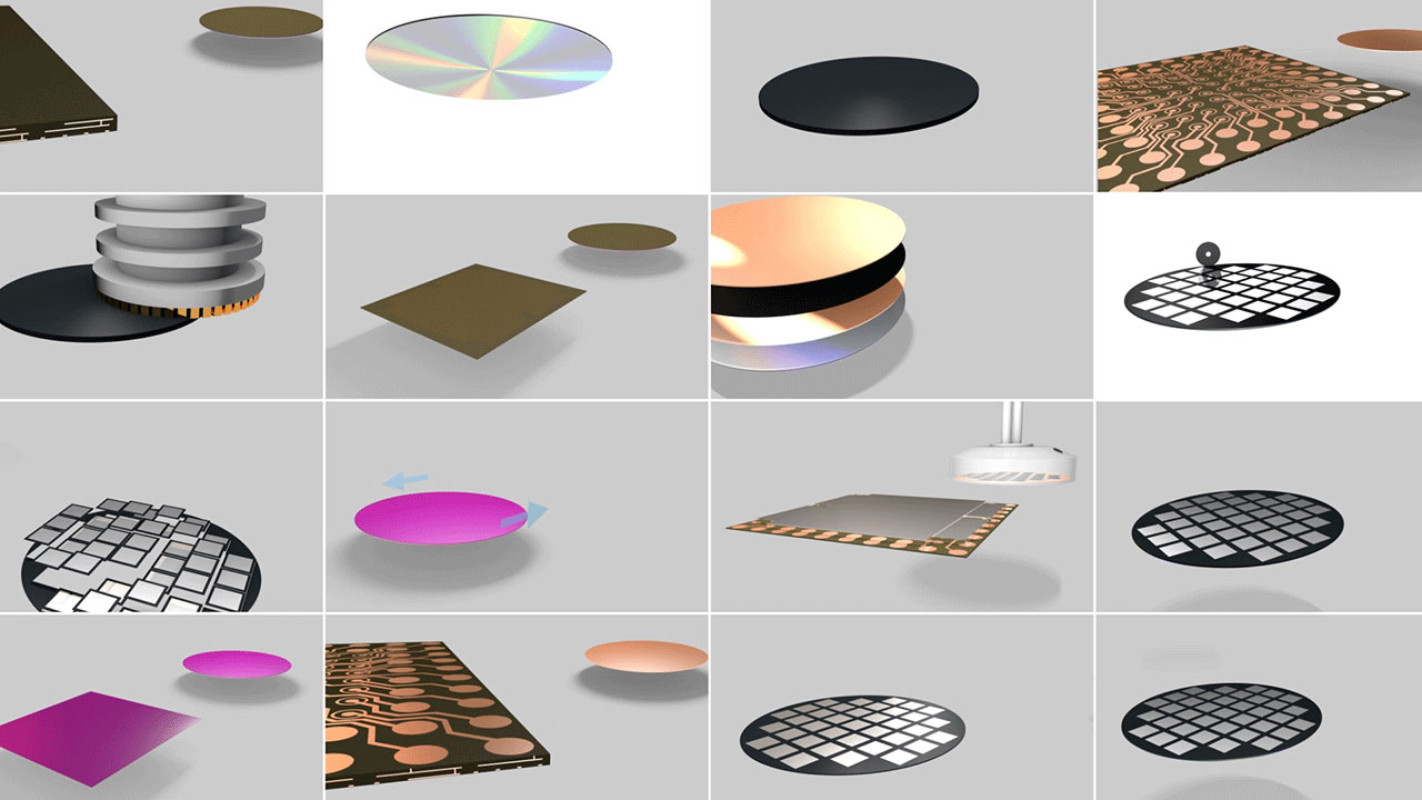
In its January 2018 news release, Mitsui Kinzoku announced the development of HRDP®, a material for the creation of ultra-fine circuits using a glass carrier for the Fan Out panel level package, based on the RDL First method2.
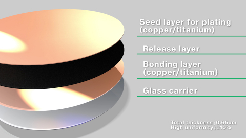
HRDP® is a special glass carrier capable of achieving high production efficiency of the Fan Out packages3, the next-generation semiconductor packaging technologies, including ultra-high density circuits designed with a line/space (L/S) ratio of 2/2 μm or less4. Currently, over 20 customers are evaluating HRDP® for commercialization.
As the first stage, mass production for a domestic multi-chip module manufacturer began in January 2021. This customer will use HRDP® to manufacture devices for the 5G market, which is expected to expand in the future, including RF modules5, and other devices for a variety of applications with plans to increase sales.
As the second stage, an overseas leading package manufacturer is planning to adopt HRDP® within FY2021.
In addition, there are plans to initiate the mass production at the other new customers for a variety of applications, such as HPC6 and mobile phones for FY2022 and onward, and the HRDP® market is expected to expand.
Under its slogan of Material Intelligence, Mitsui Kinzoku will realize customers’ wishes to ensure stable quality and sufficient supply, to provide customers with one stop solutions and to endeavor to increase its market share.
Description of Terms
1 Abbreviation of High Resolution De-bondable Panel
2 Re-Distribution Layer First method: Semiconductor chips are packaged after the process of forming the redistribution layer
3 Fan Out Package: Substrate-less packaging technology with ultra-fine re-distribution layer extended outside the chip size
4 L/S=2/2 µm: The line width of 2 µm and the space between neighboring circuit lines of 2 µm.
5 Radio Frequency Module: Product equipped with several active components (IC chips) and passive components (SAW, condenser, resistor and coil) and sealed
6 High Performance Computing: Computer with large-scale, ultra high-speed computing/processing capability
Reference
"Development of HRDP® Material for Formation of Ultra-Fine Circuits with Glass Carrier for Fan Out Panel Level Package" (Release as of January 25, 2018)
https://www.mitsui-kinzoku.com/Portals/0/resource/uploads/topics_180125e.pdf?TabModule127
Video of the RDL First method using HRDP®
https://www.youtube.com/watch?v=vHhng-NV9QA


