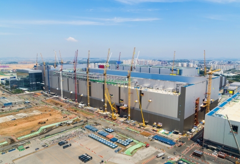
SEOUL, South Korea--(BUSINESS WIRE)--Samsung Electronics Co., Ltd., the world leader in advanced memory technology, today announced plans to expand its NAND flash production capacity in Pyeongtaek, Korea, reinforcing the company’s ability to meet demands from emerging technologies. Construction, which began this May, will pave the way for mass production of Samsung's cutting-edge V-NAND memory in the second half of 2021.
"The new investment reaffirms our commitment to sustain undisputed leadership in memory technologies, even in uncertain times," said Cheol Choi, executive vice president of Memory Global Sales & Marketing at Samsung Electronics. "We will continue to serve the market with the most optimized solutions available, while contributing to growth of the overall IT industry and the economy in general.”
In the age of the Fourth Industrial Revolution fueled by artificial intelligence, the Internet of Things and 5G expansion, the added capacity will play a major role in helping to address mid- to long-term demands for NAND flash memory. As digital lifestyles become more prevalent, Samsung will continue to be proactive in making new investments in order to seize future market opportunities.
Samsung's NAND flash production network extends from Hwaseong and Pyeongtaek in Korea to Xi'an, China. Established in 2015, Samsung's Pyeongtaek Campus is a hub for next-generation memory technologies, consisting of two of the world's largest-scale production lines.
Leveraging its significant edge in manufacturing and technology, Samsung has held the leadership position in NAND flash memory for the past 18 years, with one recent innovation being the industry-first sixth-generation (1xx-layer) V-NAND introduced last July. Through balanced investment across its global sites, Samsung aims to maintain a robust production network that will further cement its market leadership.
Reference: Samsung V-NAND mass production timeline
Date |
V-NAND |
July 2013 |
1st-generation (24-layer) 128Gb MLC V-NAND |
Aug. 2013 |
1st-generation 128Gb MLC V-NAND 960GB SSD |
Aug. 2014 |
2nd-generation (32-layer) 128Gb 3-bit V-NAND |
Sept. 2014 |
2nd-generation V-NAND SSD |
Aug. 2015 |
3rd-generation (48-layer) 256Gb 3-bit V-NAND |
Sept. 2015 |
3rd-generation V-NAND SSD '850 EVO', '950 PRO' |
Dec. 2016 |
4th-generation (64-layer) 256Gb 3-bit V-NAND |
Jan. 2017 |
4th-generation V-NAND SSD |
Jan. 2018 |
4th-generation 512Gb V-NAND 30.72TB SAS SSD |
May 2018 |
5th-generation (9x-layer) 256Gb 3-bit V-NAND |
June 2018 |
5th-generation V-NAND SSD |
June 2019 |
6th-generation (1xx-layer) 256Gb 3-bit V-NAND |
July 2019 |
6th-generation V-NAND SSD |
###
About Samsung Electronics Co., Ltd.
Samsung inspires the world and shapes the future with transformative ideas and technologies. The company is redefining the worlds of TVs, smartphones, wearable devices, tablets, digital appliances, network systems, and memory, system LSI, foundry and LED solutions. For the latest news, please visit the Samsung Newsroom at http://news.samsung.com.


