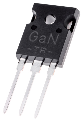
KIYOSU, Japan--(BUSINESS WIRE)--Toyoda Gosei Co., Ltd. has developed a vertical GaN power semiconductor device with high current operation of 100 amperes on a single chip, one of the highest levels yet achieved.1
Power devices are electronic components used for power conversion2 in home appliances, mobility, industry, and many other fields. The spread of electrified vehicles and renewable energy has been increasing the demand for power devices with higher performance. With the silicon used in conventional devices, however, it is difficult to significantly improve efficiency3 in converting high power.4 Toyoda Gosei has sought to overcome this with the use of GaN, a material with the physical property of high breakdown voltage, and a chip structure in which electricity flows vertically to the GaN substrate. This material and structure combination allows thinner and smaller device designs and other improvements that lead to higher performance.5
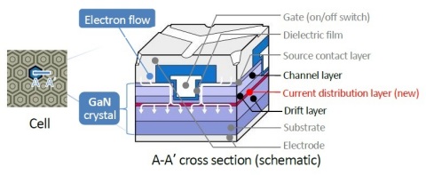
The company’s latest development, which has doubled the electric current capacity from the previous 50 amperes to 100 amperes on a single chip, is the introduction of a new current distribution layer that lowers electric resistance by expanding the flow of electricity on the drift layer. This new technology was presented at the 31st IEEE International Symposium on Power Semiconductor Devices and ICs (ISPSD) held in Shanghai, China in May 19-23, 2019.
Toyoda Gosei will continue improving the reliability and other qualities of the devices for their early commercialization in collaboration with manufacturers in the field of power electronics.
| 1 | Gallium nitride (GaN) is also a main material in blue LEDs and the company has taken advantage of the crystallizing and other techniques with GaN that it has accumulated over 30 years of development and manufacture of blue LEDs. | ||||
| 2 | Power devices convert electric voltage, current, and frequency with on/off switching and other functions. | ||||
| 3 | Efficient conversion means less power loss from change into heat during conduction and switching. | ||||
| 4 | After half a century of improvements, the balance between high breakdown voltage and low electrical resistance is approaching its limits due to the physical properties of silicon. This makes it difficult to achieve further significant reductions in conduction loss during high power operation and switching loss during high frequency operation. | ||||
| 5 | The breakdown voltage of GaN is more than 10 times greater than that of silicon. Thus, conduction loss can be reduced with thinner, lower resistance semiconductors. In addition, with a vertical structure, the entire chip is used in current flow, which makes it possible to make semiconductors smaller and reduce switching loss. With this combination, Toyoda Gosei has achieved high breakdown voltage (1.2kV level) and low resistance (1.8mΩcm2), and high frequency operation (≥10MHz). | ||||


