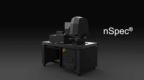
SAN FRANCISCO--(BUSINESS WIRE)--Nanotronics, an innovator in AI-enhanced industrial inspection and automation, is adding Photoluminescence Imaging to its advanced industrial inspection tool, nSpec®.
The last several years have seen the rapid adoption of new technologies that converge super-resolution optical microscopy and AI analysis. Nanotronics is at the forefront of bringing these technologies from the lab table to the factory floor, with leading semiconductor, advanced materials, rubber, automotive, and consumer electronics partners.
“Kyma’s nSpec® was purchased in 2013 and quickly became a workhorse for us, providing invaluable characterization of the properties of every wafer that goes through our facility, including wide-bandgap and ultra-wide bandgap semiconductor materials, crystalline metal films, and large-area graphene templates,” says Keith Evans, President and CEO of Kyma Technolgies. “The complex-yet-rapid AI-enabled analysis helps us learn faster and will become even more important with the addition of Photoluminescence capability.”
Detection and classification of defects and devices on semiconductors has commonly been used for process control and quality control. Now, utilizing advances in Artificial intelligence, an inspection framework can be expanded beyond a reliable tool for identifying problems, and to begin assigning casualty.
“The integration of Photoluminescence and novel AI methods into the standard nSpec® inspection system allows for rapid, adaptable detection, classification, and analysis of stacking faults in silicon carbide and other responsive materials,” explains Vadim Pinskiy, Nanotronics VP of R&D.
Combined with AI, Photoluminescence Imaging enables quantification and categorization of defects that conventional Brightfield microscopy overlooks. Photoluminescence enables the characterization of stacks and folds in SiC that cannot be seen by other methods as quickly. Using diffused light at the wavelength of the material bandgap, it not only provides a precise measurement, but one that scales faster than any laser-based method.
“Nanotronics’ nSpec® systems are a smart addition to an arsenal of oxide epi-wafer quality control instruments,” says David Rogers, Director of Nanovation. “They are economical, non-destructive tools that provide rapid quantitative full-wafer mapping of topological, defect, and optical properties...with the option of extending down to sub-optical wavelengths.”
The addition of PL imaging will provide a way to test functionality on the same wafer or product, and potentially at the same time as routine classification, giving a robust single station for solving production problems and leading to faster design iteration.
Nanotronics is presenting a paper, “Inspection and Functionality Convergence,” at SPIE Photonics West on Thursday, February 7 in room 302 at 8:30 am.
About Nanotronics
Nanotronics is an industrial platform that enables the factory of the future, where products are invented, engineered, and produced under one roof. Using AI and other advanced technologies for optical inspection, Nanotronics accelerates R&D into production, while reducing waste and creating smaller factories. Building on its legacy of revolutionizing industrial inspection for the most advanced manufacturers in nanotechnology, semiconductors, aerospace, and health, Nanotronics is at the forefront of redefining the manufacturing process. To learn more visit https://nanotronics.co.


