SEOUL, South Korea--(BUSINESS WIRE)--Samsung Electronics Co., Ltd., a world leader in advanced semiconductor technology, today introduced its new 'ISOCELL Plus' technology, which allows CMOS image sensors to capture more light, significantly increasing light sensitivity and color fidelity. Smartphone consumers can now expect even more accurate and clearer photos in challenging light environments.
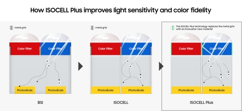
To take high-quality photographs, CMOS image sensors need to hold as much light, or photons, as possible and transmit the right color information to the photodiode. Such requirements were resolved by the introduction of Samsung’s ISOCELL technology in 2013. ISOCELL forms a physical barrier between the neighboring pixels, reducing color crosstalk and expanding the full-well capacity. This enables each pixel to absorb and hold more light than the conventional backside-illuminated (BSI) image sensor design for superior image quality.
With the introduction of ISOCELL Plus, Samsung pushes pixel isolation technology to a new level through an optimized pixel architecture. In the existing pixel structure, metal grids are formed over the photodiodes to reduce interference between the pixels, which can also lead to some optical loss as metals tend to reflect and/or absorb the incoming light. For ISOCELL Plus, Samsung replaced the metal barrier with an innovative new material developed by Fujifilm, minimizing optical loss and light reflection.
“We value our strategic relationship with Samsung and would like to congratulate on the completion of the ISOCELL Plus development,” said Naoto Yanagihara, corporate vice president of Fujifilm. “This development is a remarkable milestone for us as it marks the first commercialization of our new material. Through continuous cooperation with Samsung, we anticipate to bring more meaningful innovation to mobile cameras.”
The new ISOCELL Plus delivers higher color fidelity along with up to a 15-percent enhancement in light sensitivity. The technology also enables image sensors to equip 0.8-micrometer (µm) and smaller-sized pixels without any loss in performance, making it an optimal solution for developing super-resolution cameras with over 20 megapixels.
“Through close collaboration with Fujifilm, an industry leader in imaging and information technology, we have pushed the boundaries of CMOS image sensor technology even further,” said Ben K. Hur, vice president of System LSI marketing at Samsung Electronics. “The ISOCELL Plus will not only enable the development of ultra-high-resolution sensors with incredibly small pixel dimensions, but also bring performance advancements for sensors with larger pixel designs.”
The ISOCELL Plus will be showcased at the Mobile World Congress Shanghai, held from June 27 to 29.
About Samsung Electronics Co., Ltd.
Samsung inspires the world and shapes the future with transformative ideas and technologies. The company is redefining the worlds of TVs, smartphones, wearable devices, tablets, digital appliances, network systems, and memory, system LSI, foundry and LED solutions. For the latest news, please visit the Samsung Newsroom at http://news.samsung.com.


