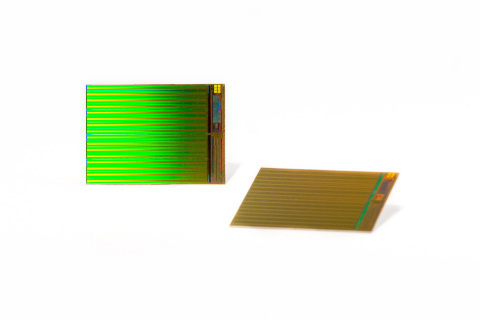
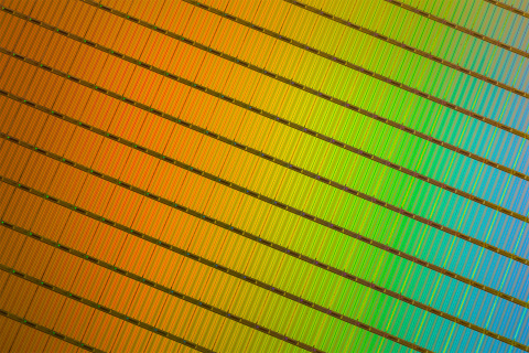
BOISE, Idaho & SANTA CLARA, Calif.--(BUSINESS WIRE)--Micron Technology, Inc. (Nasdaq: MU), and Intel Corporation today revealed the availability of their 3D NAND technology, the world’s highest-density flash memory. Flash is the storage technology used inside the lightest laptops, fastest data centers, and nearly every cellphone, tablet and mobile device.
This new 3D NAND technology, which was jointly developed by Intel and Micron, stacks layers of data storage cells vertically with extraordinary precision to create storage devices with three times higher capacity1 than competing NAND technologies. This enables more storage in a smaller space, bringing significant cost savings, low power usage and high performance to a range of mobile consumer devices as well as the most demanding enterprise deployments.
Planar NAND flash memory is nearing its practical scaling limits, posing significant challenges for the memory industry. 3D NAND technology is poised to make a dramatic impact by keeping flash storage solutions aligned with Moore’s Law, the trajectory for continued performance gains and cost savings, driving more widespread use of flash storage.
“Micron and Intel’s collaboration has created an industry-leading solid-state storage technology that offers high density, performance and efficiency and is unmatched by any flash today,” said Brian Shirley, vice president of Memory Technology and Solutions at Micron Technology. “This 3D NAND technology has the potential to create fundamental market shifts. The depth of the impact that flash has had to date—from smartphones to flash-optimized supercomputing—is really just scratching the surface of what’s possible.”
“Intel’s development efforts with Micron reflect our continued commitment to offer leading and innovative non-volatile memory technologies to the marketplace,” said Rob Crooke, senior vice president and general manager, Non-Volatile Memory Solutions Group, Intel Corporation. “The significant improvements in density and cost enabled by our new 3D NAND technology innovation will accelerate solid-state storage in computing platforms.”
Innovative Process Architecture
One of the most significant aspects of this technology is in the foundational memory cell itself. Intel and Micron chose to use a floating gate cell, a universally utilized design refined through years of high-volume planar flash manufacturing. This is the first use of a floating gate cell in 3D NAND, which was a key design choice to enable greater performance and increase quality and reliability.
The new 3D NAND technology stacks flash cells vertically in 32 layers to achieve 256Gb multilevel cell (MLC) and 384Gb triple-level cell (TLC) die that fit within a standard package. These capacities can enable gum stick-sized SSDs with more than 3.5TB of storage and standard 2.5-inch SSDs with greater than 10TB. Because capacity is achieved by stacking cells vertically, the individual cell dimensions can be considerably larger. This is expected to increase both performance and endurance and make even the TLC designs well-suited for data center storage.
The key product features of this 3D NAND design include:
- Large Capacities –Three times the capacity of existing 3D technology1—up to 48GB of NAND per die—enabling three-fourths of a terabyte to fit in a single fingertip-sized package.
- Reduced Cost per GB – First-generation 3D NAND is architected to achieve better cost efficiencies than planar NAND.
- Fast – High read/write bandwidth, I/O speeds and random read performance.
- Green – New sleep modes enable low-power use by cutting power to inactive NAND die (even when other die in the same package are active), dropping power consumption significantly in standby mode.
- Smart – Innovative new features improve latency and increase endurance over previous generations, and also make system integration easier.
The 256Gb MLC version of 3D NAND is sampling with select partners today, and the 384Gb TLC design will be sampling later this spring. The fab production line has already begun initial runs, and both devices will be in full production by the fourth quarter of this year. Both companies are also developing individual lines of SSD solutions based on 3D NAND technology and expect those products to be available within the next year.
Micron
Take part in Micron’s social conversations where we’re talking all things storage and memory:
- Media Kit: www.micron.com/about/news-and-events/media-relations/media-kits/3d-nand-media-kit
- Innovations Blog: www.micronblogs.com
- Twitter*: www.twitter.com/micronstorage
- YouTube*: www.youtube.com/microntechnology
Intel
Contribute to the SSD conversations through Intel’s social channels:
- IT Peer Network Blogs: communities.intel.com/community/itpeernetwork/blog
- Facebook*: www.facebook.com/Intel
- Twitter*: www.twitter.com/IntelSSD
- YouTube*: www.youtube.com/user/channelintel
About Micron Technology, Inc.
Micron Technology, Inc., is a global leader in advanced semiconductor systems. Micron’s broad portfolio of high-performance memory technologies—including DRAM, NAND and NOR Flash—is the basis for solid state drives, modules, multichip packages and other system solutions. Backed by more than 35 years of technology leadership, Micron’s memory solutions enable the world’s most innovative computing, consumer, enterprise storage, networking, mobile, embedded and automotive applications. Micron's common stock is traded on the NASDAQ under the MU symbol. To learn more about Micron Technology, Inc., visit www.micron.com
About Intel
Intel (NASDAQ: INTC) is a world leader in computing innovation. The company designs and builds the essential technologies that serve as the foundation for the world’s computing devices. As a leader in corporate responsibility and sustainability, Intel also manufactures the world’s first commercially available “conflict-free” microprocessors. Additional information about Intel is available at newsroom.intel.com and blogs.intel.com, and about Intel’s conflict-free efforts at conflictfree.intel.com.
________________________________________________________________________________
©2015 Micron Technology, Inc. All rights reserved. Micron and the Micron
orbit logo are trademarks of Micron Technology, Inc.
Intel is a
trademark of Intel Corporation in the United States and other countries.
*All
other trademarks are the property of their respective owners.
This document contains forward looking statements. Forward looking statements are predictions, projections and other statements about future events that are based on current expectations and assumptions and, as a result, are subject to risks and uncertainties. Many factors could cause actual results to differ materially from the forward-looking statements in this document. A detailed discussion of the factors that could affect Intel’s results and plans is included in Intel’s SEC filings, including the annual report on Form 10-K.
___________________________________________
1 Capacity difference based on comparison between Micron and Intel 384 Gb TLC 3D NAND die and other industry 3D NAND TLC


