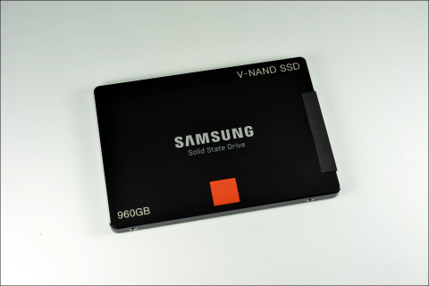
SANTA CLARA, Calif.--(BUSINESS WIRE)--Samsung Electronics Co., Ltd., the world leader in advanced memory technology, today introduced the first solid state drive (SSD) based on its industry-leading 3D V-NAND technology. Samsung announced its new SSD, designed for use in enterprise servers and data centers, during a keynote at the Flash Memory Summit 2013 here.
“By applying our 3D V-NAND – which has overcome the formidable hurdle of scaling beyond the 10-nanometer (nm) class*, Samsung is providing its global customers with high density and exceptional reliability, as well as an over 20 percent performance increase and an over 40 percent improvement in power consumption,” said E.S. Jung, executive vice president, semiconductor R&D center at Samsung Electronics and a keynote speaker at the Flash Memory Summit. “As we pioneer a new era of memory technology, we will continue to introduce differentiated green memory products and solutions for the server, mobile and PC markets to help reduce energy waste and to create greater shared value in the enterprise and for consumers.”
Samsung’s V-NAND SSD comes in 960 gigabyte (GB) and 480GB versions. The 960GB version boasts the highest level of performance, offering more than 20 percent increase in sequential and random write speeds by utilizing 64 dies of MLC 3D V-NAND flash, each offering 128 gigabits (Gb) of storage, with a six-gigabit-per-second SATA interface controller. The new V-NAND SSD also offers 35K program erase cycles and is available in a 2.5 inch form factor with x, y and z-heights of 10cm, 7cm and 7mm, which provides server manufacturers with more design flexibility and scalability.
Samsung’s proprietary 3D V-NAND technology achieves manufacturing productivity improvements over twice that of 20nm-class* planar NAND flash, by using cylinder-shaped 3D Charge Trap Flash cell structures and vertical interconnect process technology to link the 24 layers comprising the 3D cell array. During his keynote remarks, EVP E.S. Jung emphasized that “The 3D V-NAND will drive disruptive innovation that can be compared to a Digital Big Bang in the global IT industry, and contribute to much more significant growth in the memory market.”
Samsung will continue to introduce next-generation V-NAND products with enhanced performance to meet diverse customer needs for NAND flash-based storage. These customer focuses will range from large data centers that can realize higher investment potential based on greater performance and energy efficiency to PC applications that place a high priority on cost-effectiveness and high density, further strengthening Samsung’s business competitiveness.
Samsung said it began producing its new V-NAND SSDs earlier this month.
About Samsung Electronics Co., Ltd.
Samsung Electronics Co., Ltd. is a global leader in technology, opening new possibilities for people everywhere. Through relentless innovation and discovery, we are transforming the worlds of televisions, smartphones, personal computers, printers, cameras, home appliances, LTE systems, medical devices, semiconductors and LED solutions. We employ 236,000 people across 79 countries with annual sales exceeding US$187.8 billion. To discover more, please visit www.samsung.com.
* Editors’ Note: 10 nm-class means a process technology node somewhere between 10 and 20 nanometers, and 20 nm-class means a process technology node somewhere between 20 and 30 nanometers.


