
")
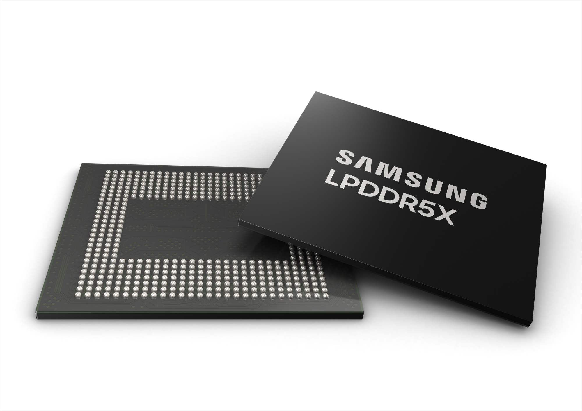
SEOUL, South Korea--(BUSINESS WIRE)--Samsung Electronics Co., Ltd., the world leader in advanced memory technology, today announced it has begun mass production for the industry’s thinnest 12 nanometer (nm)-class, 12-gigabyte (GB) and 16GB LPDDR5X DRAM packages, solidifying its leadership in the low-power DRAM market.
Leveraging its extensive expertise in chip packaging, Samsung is able to deliver ultra-slim LPDDR5X DRAM packages that can create additional space within mobile devices, facilitating better airflow. This supports easier thermal control, a factor that is becoming increasingly critical especially for high-performance applications with advanced features such as on-device AI.
"Samsung’s LPDDR5X DRAM sets a new standard for high-performance on-device AI solutions, offering not only superior LPDDR performance but also advanced thermal management in an ultra-compact package," said YongCheol Bae, Executive Vice President of Memory Product Planning at Samsung Electronics. "We are committed to continuous innovation through close collaboration with our customers, delivering solutions that meet the future needs of the low-power DRAM market."
With the new LPDDR5X DRAM packages, Samsung offers the industry’s thinnest 12 nm-class LPDDR DRAM in a 4-stack structure1, reducing the thickness by approximately 9% and improving heat resistance by about 21.2%, compared to the previous generation product.
By optimizing printed circuit board (PCB) and epoxy molding compound (EMC)2 techniques, the new LPDDR DRAM package is as thin as a fingernail at 0.65 millimeters (mm), the thinnest among existing LPDDR DRAM of 12GB or above. Samsung’s optimized back-lapping3 process is also used to minimize the package height.
Samsung plans to continue expanding the low-power DRAM market by supplying its 0.65mm LPDDR5X DRAM to mobile processor makers as well as mobile device manufacturers. As demand for high-performance, high-density mobile memory solutions in smaller package sizes continues to grow, the company plans to develop 6-layer 24GB and 8-layer 32GB modules into the thinnest LPDDR DRAM packages for future devices.
About Samsung Electronics Co., Ltd.
Samsung inspires the world and shapes the future with transformative ideas and technologies. The company is redefining the worlds of TVs, smartphones, wearable devices, tablets, home appliances, network systems, and memory, system LSI, foundry and LED solutions, and delivering a seamless connected experience through its SmartThings ecosystem and open collaboration with partners. For the latest news, please visit the Samsung Newsroom at news.samsung.com
1 Structure with four layers packaged together, and each layer consists of two LPDDR DRAMs.
2 Material that protects semiconductor circuits from various external environments such as heat, impacts, and moisture.
3 Grinding the backside of a wafer.