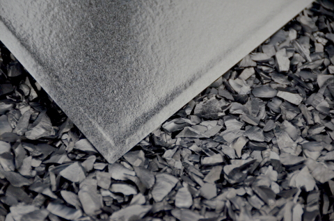
BEDFORD, Mass.--(BUSINESS WIRE)--1366 Technologies (“1366”) today unveiled the first of a series of R&D achievements that have the potential to change the way the solar industry thinks about wafer features. The company’s proprietary Direct Wafer process has demonstrated the ability to grow a “three dimensional” wafer or a thin wafer with a thick border, an advancement impossible with conventional ingot-based production technologies. The 3D feature further reduces the amount of silicon required for each wafer without sacrificing strength, durability or performance. It also allows the dominant crystalline silicon PV supply chain to lower costs while leveraging its existing infrastructure.
“The unique capabilities of our Direct Wafer process are an enabler for the crystalline silicon industry to continue its dominant market share position and deliver progressively lower-cost PV solutions for years to come,” said Frank van Mierlo, CEO, 1366 Technologies. “The 3D wafer feature allows us to meet the industry’s anticipated need for thinner wafers without compromising existing standards or asking manufacturers to abandon their existing manufacturing lines.”
To decrease the amount of silicon used by photovoltaic wafers, manufacturers have long pursued methods to reduce wafer thickness. While wire sawing can be used to produce wafers thinner than the standard 180-200 micron thickness, these thin wafers have reduced mechanical integrity and break during cell fabrication, electrical interconnection and encapsulation in modules. As such, standard industry wafer thickness has remained between 180-200 microns. 1366’s Direct Wafer process has the unique ability to locally-control wafer thickness and provide standard 180-200 micron thickness in stress-critical areas such as wafer perimeter or ribs where busbar soldering will occur, while reducing thickness to 100-120 microns for the remainder of the wafer. The result cuts silicon consumption to ~1.5 g/W and creates a strong, thin wafer able to withstand typical manufacturing stresses.
“The beauty of our Direct Wafer process is that the innovation begets further innovation,” continued van Mierlo. “The ability to access the wafer surface during growth is a tremendous advantage and the source of more innovation to come.”
1366’s Direct Wafer technology is a transformative manufacturing process that offers significant advantages over traditional ingot-based wafer production technologies, including the ability to introduce new wafer features that reduce cost and increase efficiency. The process makes wafers in a single step, pulling them directly from molten silicon instead of today’s multi-step, energy- and capital-intensive approach, resulting in significant wafer production cost savings.
ABOUT 1366 TECHNOLOGIES
1366
Technologies aims to deliver solar at a cost less than coal. The company
combines breakthrough technology innovations with lean manufacturing
processes to make a new class of silicon wafers, the building blocks of
solar cells, at a fraction of today’s cost. Developed by a veteran team
of scientists, engineers and entrepreneurs, the company’s novel approach
breaks the historic efficiency and cost tradeoffs of photovoltaics. 1366
Technologies is headquartered in Bedford, MA. For more information,
please visit www.1366tech.com.


