SEOUL, South Korea--(BUSINESS WIRE)--Samsung Electronics Co., Ltd., a world leader in advanced component solutions, today introduced advanced chip scale packaging (CSP) technology for use in a diversity of LED lighting applications at LIGHTFAIR International 2015, being held in New York, May 5-7.
Samsung’s new CSP technology significantly scales down the size of an LED package, which enables more flexible and compact designs when manufacturing consumer LED lighting modules or fixtures, and lowers the manufacturing and operational costs of a LED lighting system. Samsung’s CSP also provides flexibility in adjusting the size of the light-emitting surface and the luminance level, to meet the differing requirements of various lighting fixture applications.
“Our LED chip scale packaging technology will contribute to providing innovative LED component solutions that can overcome the limitations of today's LED lighting market,” said Dr. Jacob Tarn, Executive Vice President, LED Lighting Business Team, Samsung Electronics. “We will incorporate the new technology in future Samsung LED products and continue to introduce more advanced LED technology, while strengthening our presence in the global LED market."
The newly introduced CSP technology is actually Samsung’s second generation. Last year, Samsung introduced LED package products using its first chip scale packaging technology which featured a versatile new type of flip chip packaging. The first generation CSP was created by flipping over blue LED chips and then adhering a phosphor film to each of them. Unlike conventional LED packages that require a packaging process following the actual chip manufacturing, this allowed chip-scale packages to be created without a mold, enabling more compact LED lighting designs.
Samsung’s new, second generation CSP takes the advancements even further. In the second generation CSP, blue LED chips are flipped over and immediately coated with a phosphor substance. The second generation CSP has inherited the advantages of the first generation CSPs, such as freedom from metal wires and plastic molds, which lead to smaller packages, more compact lighting designs, lower thermal resistance and high current availability, resulting in high flux and greater reliability. In addition, using the second generation CSP process makes new Samsung LED packages even more competitive in raw costs, and achieves higher robustness and reliability with a longer life span, as well as higher operating temperatures and current.
Based on the new advancements, Samsung’s second generation CSP technology enables LED packages with an ultra-compact form factor: 1.2mm by 1.2mm. These dimensions are approximately 30 percent smaller than the 1.4mm by 1.4mm measure of the first generation CSP, while offering a 10 percent improvement in light performance. It also provides higher light quality with advanced multifaceted phosphor coating technology, which covers the top and four sides of an LED package with phosphor. Because of the small form factor that it allows, the new CSP technology can be used in a wide variety of LED packages for applications that range from ambient light and spotlight, to downlight and bulb lighting.
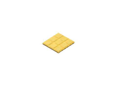
Moreover, the second generation CSP LED packages can bring even greater design flexibility by offering added delivery options. In the manufacturing process, 2 by 2 and 3 by 3 CSP arrays can be easily created and offered to customers, depending on a diversity of market needs. The availability of CSP arrays provides not only more design flexibility, but also better light quality in each LED luminaire through their one-lens design, in which the CSP arrays share a single lens instead of having to use individual lenses for multiple conventional packages.
Samsung’s ultra-compact, second generation CSP technology is expected to be applied to new LED packages slated to be introduced in the fourth quarter of this year, and will support a wide range of Correlated Color Temperature (CCT) specifications.
At LIGHTFAIR International 2015, Samsung will showcase the vast majority of its LED component product lineups at booth #521 in the Jacob Javits Convention Center.
About Samsung Electronics Co., Ltd.
Samsung Electronics Co., Ltd. inspires the world and shapes the future with transformative ideas and technologies, redefining the worlds of TVs, smartphones, wearable devices, tablets, cameras, digital appliances, printers, medical equipment, network systems, and semiconductor and LED solutions. We are also leading in the Internet of Things space through, among others, our Smart Home and Digital Health initiatives. We employ 307,000 people across 84 countries with annual sales of US $196 billion. To discover more, please visit our official website at www.samsung.com and our official blog at global.samsungtomorrow.com


