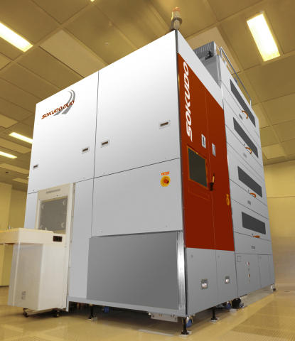
ALBANY, N.Y. & KYOTO, Japan--(BUSINESS WIRE)--Dainippon Screen Mfg. has confirmed our subsidiary company’s SOKUDO DUO 450mm coat/develop track system has been chosen by the Global 450mm Consortium (G450C), headquartered at the SUNY College of Nanoscale Science and Engineering (CNSE) in Albany, New York, for immersion ArF lithography and Directed Self-Assembly (DSA) applications. The SOKUDO DUO will be added to Dainippon Screen’s suite of 450mm cleaning equipment in CNSE’s NanoFab Xtension. Dainippon Screen’s 450mm wafer scrubber, single wafer cleaning, as well as millisecond annealing system will be among the equipment set to be available for the G450C, a public-private partnership announced by New York Governor Andrew M. Cuomo in September 2011 to facilitate the industry’s transition to the new, standard 450mm wafer size. The consortium is spearheaded by CNSE in partnership with Intel, IBM, GLOBALFOUNDRIES, Samsung, and TSMC.
The SOKUDO DUO will be interfaced in-line with a 450mm immersion ArF lithography system and will arrive at the G450C headquarters in Albany, NY, in the summer of 2014, when installation and characterization will begin. This complements and supports the July 2013 New York State announcement that a 450mm wafer ArF immersion lithography system is scheduled for delivery to CNSE in April 2015. As part of the agreement with the G450C, notably, SOKUDO will also provide 450mm virtual fab track process support to enable 450mm DSA-patterned test wafer production for G450C member equipment development. The DSA patterning capability will also be integrated into the SOKUDO DUO for complementary lithography with immersion ArF exposures.
“We are very pleased to be aligned with the G450C, in New York State, and its member companies, who are pioneering the 450mm wafer transition,” noted Tadahiro Suhara, CEO of SOKUDO Co., Ltd. and President of Dainippon Screen’s Semiconductor Equipment Company. “The depth of the Dainippon Screen group’s involvement in the G450C is a testament to our leadership position in 450mm semiconductor manufacturing equipment development. I am particularly proud of the SOKUDO DUO 450mm track system selection, to solidify our role as a leading-edge track supplier for the long term.”
“Under the leadership and vision of Governor Andrew Cuomo, New York is firmly established as the hub for the critical industry transition to 450mm wafer technology,” said Paul Farrar, Jr., CNSE Vice President for Manufacturing Innovation and General Manager of the G450C. “We are happy to continue our partnership with Dainippon Screen’s Semiconductor Equipment Company and welcome their subsidiary, SOKUDO Co., Ltd. to help in enabling the important transition to 450mm technology.”
At the SEMICON West SOKUDO Lithography Breakfast Forum in July 2013, it was revealed that a full 450mm wafer scale up of the SOKUDO DUO has been in operation for more than one year within the Dainippon Screen’s Process Technology Center (Hikone, Japan) clean room. SOKUDO was among the first companies to significantly support the consortium with various 450mm thin film coated test wafers, including adhesion layer coatings for 450mm nanoimprint lithography patterning and DSA capabilities and characterization.
As leading companies in semiconductor equipment, Dainippon Screen and SOKUDO will continue to deliver world-class products and contribute to the development of the industry.
About Dainippon Screen Mfg. Co., Ltd.
Dainippon Screen was established in 1943 and is currently one of the top 10 suppliers of semiconductor equipment, including wafer cleaning and annealing systems. It has expanded its base with core image processing, lithography, and cleaning technologies developed over the years, including businesses in flat panel display, printed circuit board, and media technologies. URL: www.screen.co.jp/eng/
About SOKUDO Co., Ltd.
SOKUDO is a subsidiary company of Dainippon Screen focused on advanced coat/develop track systems for semiconductor manufacturing. SOKUDO’s line of products serve a full range of lithography applications (such as i-line, KrF, immersion ArF, EUV, E-Beam), as well as various niche markets covering the 50 to 450 mm substrate size range. URL: www.sokudo.com
About SUNY CNSE
The SUNY College of Nanoscale Science and Engineering (CNSE) is the world leader in the emerging disciplines of nanoscience, nanoengineering, nanobioscience, and nanoeconomics. CNSE represents the world’s most advanced university-driven research enterprise, with more than $20 billion in high-tech investments and over 300 corporate partners. The 1.3 million-square-foot Albany NanoTech megaplex is home to more than 3,100 scientists, researchers, engineers, students, and faculty. URL: www.sunycnse.com


