Newsroom
Sorted by: Latest
-
Yamaha U.S. Marine Business Unit Earns Top Industry Honors at Miami International Boat Show®
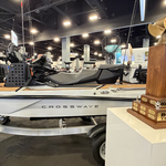
MIAMI--(BUSINESS WIRE)--Yamaha’s U.S. Marine Business Unit earned multiple top honors during the 2026 Miami International Boat Show®, reinforcing the company’s leadership in innovation, design and customer satisfaction across the marine industry. “These awards reflect the passion and precision our teams bring to every product we design and build,” said Ben Speciale, President, Yamaha U.S. Marine Business Unit. “From redefining entire categories with the CrossWave to delivering customer satisfac...
-
Pizza City Fest Returns to L.A. LIVE With 40 of Southern California’s Top Pizzerias, April 25-26, 2026
LOS ANGELES--(BUSINESS WIRE)--PIZZA CITY FEST RETURNS TO L.A. LIVE WITH 40 OF SOUTHERN CALIFORNIA’S TOP PIZZERIAS, APRIL 25-26, 2026...
-
FiRa Consortium Launches Ultra-Wideband Plugfests to Advance Industry Interoperability
BEAVERTON, Ore.--(BUSINESS WIRE)--The FiRa® Consortium today announced the launch of FiRa Plugfests, a new industry initiative designed to accelerate ultra-wideband (UWB) interoperability through hands-on, real-world testing and collaboration. Leading the way, FiRa Sponsor members Qualcomm Technologies and STMicroelectronics will host the first two FiRa Plugfests in 2026, providing FiRa members with dedicated venues to validate implementations, share technical insights, and strengthen confidenc...
-
Keysight Introduces PAM3 Signaling with New GDDR7 Transmitter Compliance Solution for Next-Generation Graphics Memory
SANTA ROSA, Calif.--(BUSINESS WIRE)--Keysight Technologies, Inc. (NYSE: KEYS) announced its new graphics double data rate 7 (GDDR7) transmitter compliance solution, that accelerates validation of Joint Electron Device Engineering Council (JEDEC) standards for graphics and artificial intelligence (AI) applications. Growing demand for high-performance computing, gaming, and AI platforms is driving memory and GPU vendors to adopt GDDR7, but the transition is creating significant validation challen...

-
Strike Looms at Children’s Aid Society of Toronto as Province-Wide Child Welfare Crisis Deepens
TORONTO--(BUSINESS WIRE)--CUPE Local 2316, representing workers at the Children’s Aid Society of Toronto, are officially in a legal strike position as negotiations between the union and the employer have not led to an agreement and workers warn that a broader provincial funding crisis is pushing child welfare services to the brink. Frontline and support staff say chronic understaffing, rising case complexity, growing service demands, and deep program cuts are preventing them from consistently m...
-
Versa Named SASE Industry Leader and Outperformer for Second Consecutive Year
SANTA CLARA, Calif.--(BUSINESS WIRE)--Versa, the global leader in unified security and networking, today announced that GigaOm, an enterprise technology research firm, has rated Versa Unified SASE an industry leader and outperformer for the second consecutive year in its annual competitive report, GigaOm Radar for Secure Access Service Edge (SASE). In the report, 17 vendors are classified as leaders, challengers, or entrants based on scoring across 24 technical and business criteria, with Versa...
-
Sysdig Named a Leader in CNAPP as Runtime Redefines Cloud Security in 2026
SAN FRANCISCO--(BUSINESS WIRE)--Sysdig today announced that it has been named a Leader in “The Forrester Wave™: Cloud Native Application Protection Solutions, Q1 2026” report, earning the distinction alongside just two other companies. Out of 14 vendors evaluated, Sysdig was also one of only three cloud security providers rated above average for customer feedback, which Sysdig sees as a reflection of strong customer trust as organizations continue to realize increasing value from Sysdig’s runti...
-
KBRA Assigns Preliminary Ratings to CROSS 2026-NQM2 Mortgage Trust
NEW YORK--(BUSINESS WIRE)--KBRA assigns preliminary ratings to ten classes of mortgage pass-through certificates from CROSS 2026-NQM2 Mortgage Trust, an RMBS transaction issued under the CROSS shelf, where Hildene-CCC Loan Acquisition II, LLC and CrossCountry Capital are the co-sponsors. This $612.2 million transaction is collateralized by a pool of 1,232 residential mortgages, including a meaningful concentration of collateral that KBRA considers to be “non-prime” (71.0%), with fixed-rate mort...
-
Churchill Stateside Group Provides Private Tax-Exempt Loan (P-TEL) Financing for 4% LIHTC Developments
CLEARWATER, Fla.--(BUSINESS WIRE)--Churchill Stateside Group (CSG) is highlighting its Private Tax-Exempt Loan (P-TEL) financing platform, an established construction-to-permanent debt solution designed for 4% Low-Income Housing Tax Credit (LIHTC) developments utilizing tax-exempt bonds. The P-TEL program provides developers with a streamlined, single-source financing structure from construction through stabilization, pairing tax-exempt interest rates with long-term, fixed-rate permanent financ...
-
First Northern Bank Acquires Beacon Wealth Strategies
DIXON, Calif.--(BUSINESS WIRE)--First Northern Advisors, a division of First Northern Bank, is pleased to announce the acquisition of Beacon Wealth Strategies, a well-respected independent financial advisory firm owned and operated by Tom Cicchini. This acquisition ensures the continued delivery of personalized wealth management services to Beacon Wealth Strategies’ clients while strengthening First Northern Bank’s wealth management platform through increased assets under management. As part of...